Visible to Intel only — GUID: rut1510104154035
Ixiasoft
1. About the High Bandwidth Memory (HBM2) Interface Intel® FPGA IP
2. Introduction to High Bandwidth Memory
3. Stratix® 10 HBM2 Architecture
4. Creating and Parameterizing the High Bandwidth Memory (HBM2) Interface Intel® FPGA IP
5. Simulating the High Bandwidth Memory (HBM2) Interface Intel® FPGA IP
6. High Bandwidth Memory (HBM2) Interface Intel® FPGA IP Interface
7. High Bandwidth Memory (HBM2) Interface Intel® FPGA IP Controller Performance
8. High Bandwidth Memory (HBM2) Interface Intel® FPGA IP User Guide Archives
9. Document Revision History for High Bandwidth Memory (HBM2) Interface FPGA IP User Guide
4.2.1. General Parameters for High Bandwidth Memory (HBM2) Interface Intel® FPGA IP
4.2.2. FPGA I/O Parameters for High Bandwidth Memory (HBM2) Interface Intel® FPGA IP
4.2.3. Controller Parameters for High Bandwidth Memory (HBM2) Interface Intel® FPGA IP
4.2.4. Diagnostic Parameters for High Bandwidth Memory (HBM2) Interface Intel® FPGA IP
4.2.5. Example Designs Parameters for High Bandwidth Memory (HBM2) Interface Intel® FPGA IP
4.2.6. Register Map IP-XACT Support for HBM2 IP
5.1. High Bandwidth Memory (HBM2) Interface Intel® FPGA IP Example Design
5.2. Simulating High Bandwidth Memory (HBM2) Interface Intel® FPGA IP with ModelSim* and Questa*
5.3. Simulating High Bandwidth Memory (HBM2) Interface Intel® FPGA IP with Synopsys VCS*
5.4. Simulating High Bandwidth Memory (HBM2) Interface Intel® FPGA IP with Riviera-PRO*
5.5. Simulating High Bandwidth Memory (HBM2) Interface Intel® FPGA IP with Cadence Xcelium* Parallel Simulator
5.6. Simulating High Bandwidth Memory (HBM2) Interface Intel® FPGA IP for High Efficiency
5.7. Simulating High Bandwidth Memory (HBM2) Interface IP Instantiated in Your Project
6.1. High Bandwidth Memory (HBM2) Interface Intel® FPGA IP High Level Block Diagram
6.2. High Bandwidth Memory (HBM2) Interface Intel® FPGA IP Controller Interface Signals
6.3. User AXI Interface Timing
6.4. User APB Interface Timing
6.5. User-controlled Accesses to the HBM2 Controller
6.6. Soft AXI Switch
7.1. High Bandwidth Memory (HBM2) DRAM Bandwidth
7.2. High Bandwidth Memory (HBM2) Interface Intel® FPGA IP HBM2 IP Efficiency
7.3. High Bandwidth Memory (HBM2) Interface Intel® FPGA IP Latency
7.4. High Bandwidth Memory (HBM2) Interface Intel® FPGA IP Timing
7.5. High Bandwidth Memory (HBM2) Interface Intel® FPGA IP DRAM Temperature Readout
Visible to Intel only — GUID: rut1510104154035
Ixiasoft
5.1. High Bandwidth Memory (HBM2) Interface Intel® FPGA IP Example Design
The following illustration shows a high-level block diagram of the HBM2 example design that provides the simulation environment for the High Bandwidth Memory (HBM2) Interface Intel® FPGA IP HBM2 IP when generated for simulation.
Figure 12. High Bandwidth Memory (HBM2) Interface Intel® FPGA IP Generated for Simulation
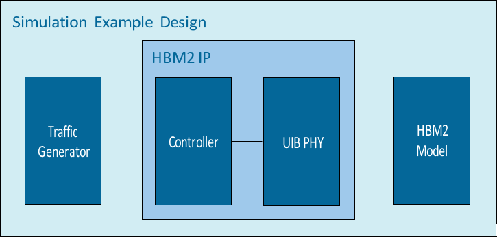
The Traffic Generator emulates a real-world application that writes to, and reads back from memory and validates the read data. You can modify the traffic generator logic to fit your traffic pattern or drive the transactions to the HBM2 memory with your own logic.
Simulation incorporates an abstract model of the hardened HBM2 controller and the universal interface block (UIB). The HBM2 controller performs data reordering and enhancement functions, and allows communication between the AXI4 user interface and the UIB PHY. The universal interface block PHY (UIB PHY) is the physical-layer interface that carries low-level signaling.
The HBM2 Model is an abstract generic model representative of the HBM2 DRAM for simulation. This is not a vendor-specific model.