Visible to Intel only — GUID: hco1416493230225
Ixiasoft
1. Functional Description—UniPHY
2. Functional Description— Intel® MAX® 10 EMIF IP
3. Functional Description—Hard Memory Interface
4. Functional Description—HPS Memory Controller
5. Functional Description—HPC II Controller
6. Functional Description—QDR II Controller
7. Functional Description—RLDRAM II Controller
8. Functional Description—RLDRAM 3 PHY-Only IP
9. Functional Description—Example Designs
10. Introduction to UniPHY IP
11. Latency for UniPHY IP
12. Timing Diagrams for UniPHY IP
13. External Memory Interface Debug Toolkit
14. Upgrading to UniPHY-based Controllers from ALTMEMPHY-based Controllers
1.1. I/O Pads
1.2. Reset and Clock Generation
1.3. Dedicated Clock Networks
1.4. Address and Command Datapath
1.5. Write Datapath
1.6. Read Datapath
1.7. Sequencer
1.8. Shadow Registers
1.9. UniPHY Interfaces
1.10. UniPHY Signals
1.11. PHY-to-Controller Interfaces
1.12. Using a Custom Controller
1.13. AFI 3.0 Specification
1.14. Register Maps
1.15. Ping Pong PHY
1.16. Efficiency Monitor and Protocol Checker
1.17. UniPHY Calibration Stages
1.18. Document Revision History
1.7.1.1. Nios® II-based Sequencer Function
1.7.1.2. Nios® II-based Sequencer Architecture
1.7.1.3. Nios® II-based Sequencer SCC Manager
1.7.1.4. Nios® II-based Sequencer RW Manager
1.7.1.5. Nios® II-based Sequencer PHY Manager
1.7.1.6. Nios® II-based Sequencer Data Manager
1.7.1.7. Nios® II-based Sequencer Tracking Manager
1.7.1.8. Nios® II-based Sequencer Processor
1.7.1.9. Nios® II-based Sequencer Calibration and Diagnostics
1.17.1. Calibration Overview
1.17.2. Calibration Stages
1.17.3. Memory Initialization
1.17.4. Stage 1: Read Calibration Part One—DQS Enable Calibration and DQ/DQS Centering
1.17.5. Stage 2: Write Calibration Part One
1.17.6. Stage 3: Write Calibration Part Two—DQ/DQS Centering
1.17.7. Stage 4: Read Calibration Part Two—Read Latency Minimization
1.17.8. Calibration Signals
1.17.9. Calibration Time
4.1. Features of the SDRAM Controller Subsystem
4.2. SDRAM Controller Subsystem Block Diagram
4.3. SDRAM Controller Memory Options
4.4. SDRAM Controller Subsystem Interfaces
4.5. Memory Controller Architecture
4.6. Functional Description of the SDRAM Controller Subsystem
4.7. SDRAM Power Management
4.8. DDR PHY
4.9. Clocks
4.10. Resets
4.11. Port Mappings
4.12. Initialization
4.13. SDRAM Controller Subsystem Programming Model
4.14. Debugging HPS SDRAM in the Preloader
4.15. SDRAM Controller Address Map and Register Definitions
4.16. Document Revision History
10.7.1. DDR2, DDR3, and LPDDR2 Resource Utilization in Arria V Devices
10.7.2. DDR2 and DDR3 Resource Utilization in Arria II GZ Devices
10.7.3. DDR2 and DDR3 Resource Utilization in Stratix III Devices
10.7.4. DDR2 and DDR3 Resource Utilization in Stratix IV Devices
10.7.5. DDR2 and DDR3 Resource Utilization in Arria V GZ and Stratix V Devices
10.7.6. QDR II and QDR II+ Resource Utilization in Arria V Devices
10.7.7. QDR II and QDR II+ Resource Utilization in Arria II GX Devices
10.7.8. QDR II and QDR II+ Resource Utilization in Arria II GZ, Arria V GZ, Stratix III, Stratix IV, and Stratix V Devices
10.7.9. RLDRAM II Resource Utilization in Arria® V Devices
10.7.10. RLDRAM II Resource Utilization in Arria® II GZ, Arria® V GZ, Stratix® III, Stratix® IV, and Stratix® V Devices
13.1. User Interface
13.2. Setup and Use
13.3. Operational Considerations
13.4. Troubleshooting
13.5. Debug Report for Arria V and Cyclone V SoC Devices
13.6. On-Chip Debug Port for UniPHY-based EMIF IP
13.7. Example Tcl Script for Running the Legacy EMIF Debug Toolkit
13.8. Document Revision History
Visible to Intel only — GUID: hco1416493230225
Ixiasoft
3.3. MPFE Signal Descriptions
The following table describes the signals for the multi-port front end.
| Signal |
Direction |
Description |
|---|---|---|
| avl_<signal_name>_# (1) |
— |
Local interface signals. |
| mp_cmd_clk_#_clk (1) |
Input |
Clock for the command FIFO buffer. (3) Follow Avalon® -MM master frequency. Maximum frequency is one-half of the interface frequency, and subject to timing closure. |
| mp_cmd_reset_n_#_reset_n (1) |
Input |
Asynchronous reset signal for command FIFO buffer. |
| mp_rfifo_clk_#_clk (2) |
Input |
Clock for the read data FIFO buffer. Follow Avalon® -MM master frequency. Maximum frequency is one-half of the interface frequency, and subject to timing closure. |
| mp_rfifo_reset_n_#_reset_n (2) |
Input |
Asynchronous reset signal for read data FIFO buffer. |
| mp_wfifo_clk_#_clk (2) |
Input |
Clock for the write data FIFO buffer. Follow Avalon® -MM master frequency. Maximum frequency is one-half of the interface frequency, and subject to timing closure. |
| mp_wfifo_reset_n_#_reset_n (2) |
Input |
Asynchronous reset signal for write data FIFO buffer. |
| bonding_in_1/2/3 |
Input |
Bonding interface input port. Connect second controller bonding output port to this port according to the port sequence. |
| bonding_out_1/2/3 |
Output |
Bonding interface output port. Connect this port to the second controller bonding intput port according to the port sequence. |
| Notes to Table:
|
||
Every input interface (command, read data, and write data) has its own clock domain. Each command port can be connected to a different clock, but the read data and write data ports associated with a command port must connect to the same clock as that command port. Each input interface uses the same reset signal as its clock.
By default, the IP generates all clock signals regardless of the MPFE settings, but all unused ports and FIFO buffers are connected to ground.
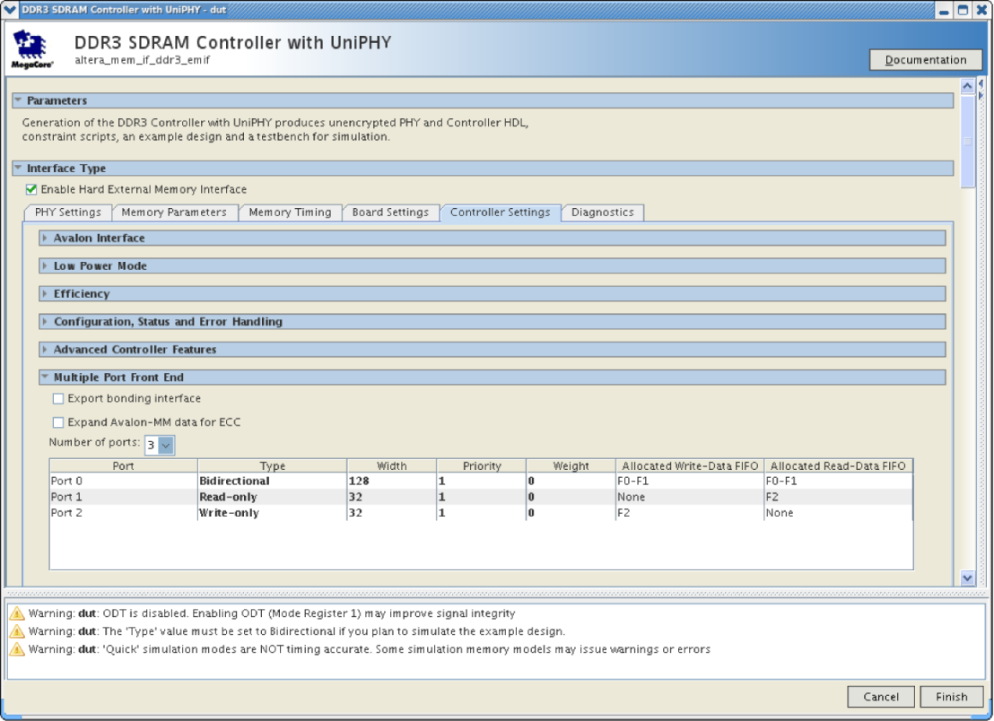
The command ports can be used only in unidirectional configurations, with either 4 write and 2 read, 3 write and 3 read, or 2 write and 4 read scenarios. For bidirectional ports, the number of clocks is reduced from 6 to a maximum of 4.
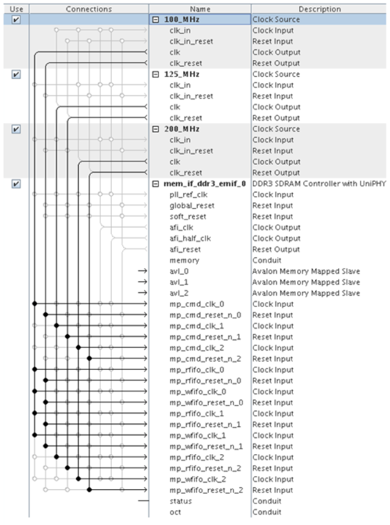
For the scenario depicted in the following figure:
- command port 0 is associated with read and write data FIFO 0 and 1
- command port 1 is associated with read data FIFO 2
- command port 2 is associated with write data FIFO 2
Figure 39. Sample MPFE Configuration
Therefore, if port 0 (avl_0) is clocked by a 100 MHz clock signal, mp_cmd_clk_0, mp_rfifo_clk_0, mp_rfifo_clk_1, mp_wfifo_clk_0, and mp_wfifo_clk_1 must all be connected to the same 100 MHz clock, as illustrated below.
Figure 40. Sample Connection Mapping