2.1. Block Descriptions
The DMA design example for the P-Tile Avalon-MM IP for PCIe includes the following components:
- DUT: The P-Tile Avalon-MM IP for PCIe Endpoint.
- MEM0: An on-chip dual-port memory that connects to the Read Data Mover and Write Data Mover interfaces of the DUT.
- DMA_CONTROLLER: A DMA Controller that interfaces with the normal and priority descriptor queues of the DUT's Read Data Mover and Write Data Mover.
- BAR_INTERPRETER: A BAR Interpreter that combines the address and BAR number to form a wider address that Platform Designer can use to route memory transactions to the various slaves. The BAR Interpreter connects the Bursting Master of the DUT to the dual-port memory.
- Reset Release IP: This IP holds the control circuit in reset until the device has fully entered user mode. The FPGA asserts the INIT_DONE output to signal that the device is in user mode. The Reset Release IP generates an inverted version of the internal INIT_DONE signal to create the nINIT_DONE output that you can use for your design.
The nINIT_DONE signal is high until the entire device enters user mode. After nINIT_DONE asserts (low), all logic is in user mode and operates normally. You can use the nINIT_DONE signal in one of the following ways:
- To gate an external or internal reset.
- To gate the reset input to the transceiver and I/O PLLs.
- To gate the write enable of design blocks such as embedded memory blocks, state machine, and shift registers.
- To synchronously drive register reset input ports in your design.
Figure 2. Platform Designer View of the x16 Endpoint DMA Design Example for the P-Tile Avalon-MM IP for PCIe
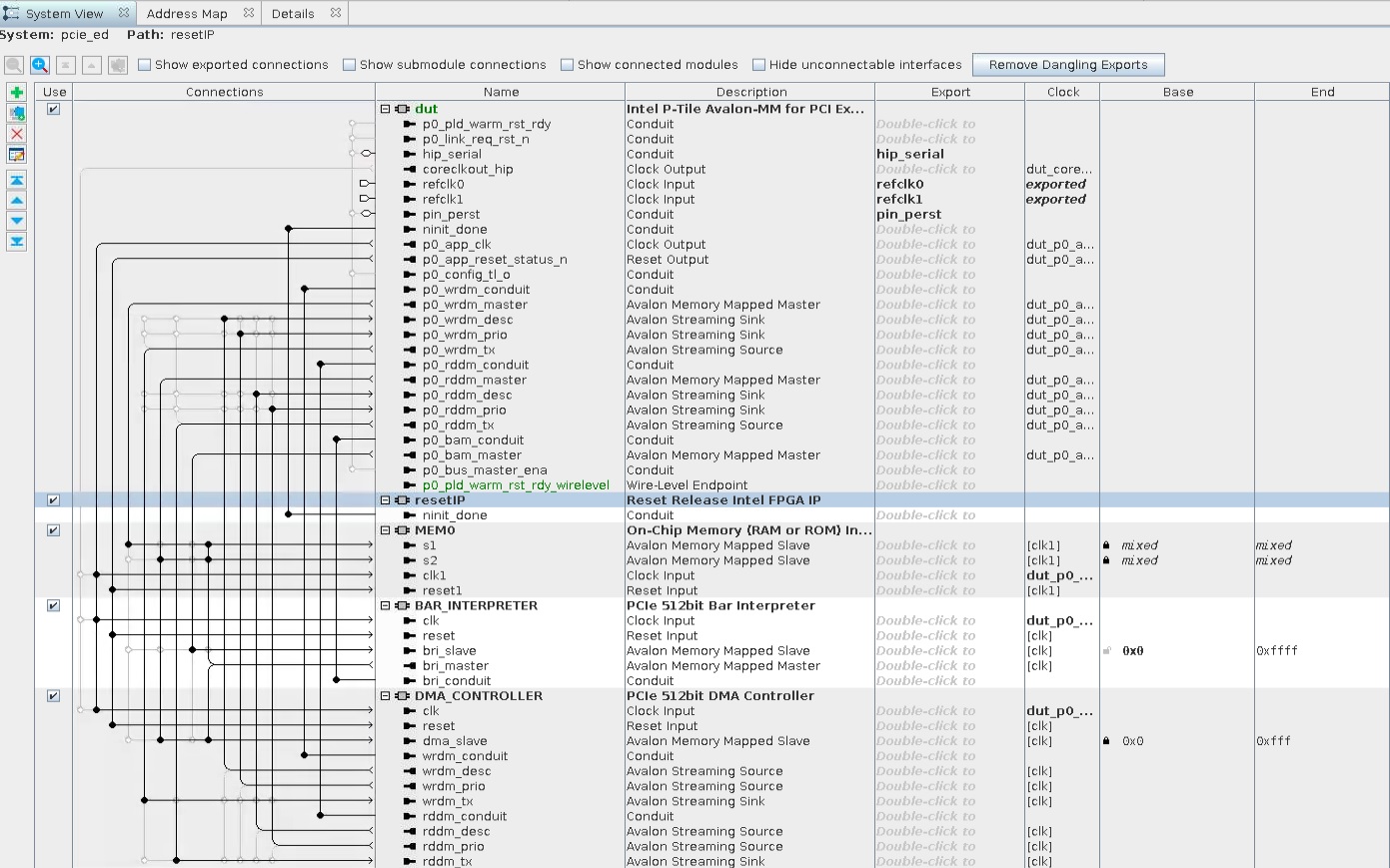
Figure 3. Platform Designer View of the x8 Endpoint DMA Design Example for the P-Tile Avalon-MM IP for PCIe

Note: Only Port 0 is used in the x8 design example.
Note: For hardware testing purpose, plug the x8 design example into a x8 slot.
| Slave | BAR_INTERPRETER.bri_master | dut.p0_wrdm_master | dut.p0_rddm_master | dut.p0_bam_master |
|---|---|---|---|---|
| BAR_INTERPRETER.bri_slave | 0x0000_0000_0000_0000 - 0x0000_0000_0000_ffff | |||
| DMA_CONTROLLER.dma_slave | 0x0000_0000 - 0x0000_0fff | 0x0000_0000_0000_0000 - 0x0000_0000_0000_0fff | ||
| MEM0.s1 | 0x0002_0000 - 0x0002_7fff | 0x0000_0000_0001_0000 - 0x0000_0000_0001_7fff | ||
| MEM0.s2 | 0x0002_8000 - 0x0002_ffff | 0x0000_0000_0001_0000 - 0x0000_0000_0001_7fff |