Visible to Intel only — GUID: tre1628558237707
Ixiasoft
1. Power Distribution Network
2. Gigahertz Channel Design Considerations
3. PCB and Stack-Up Design Considerations
4. Device Pin-Map, Checklists, and Connection Guidelines
5. General Board Design Considerations/Guidelines
6. Memory Interfacing Guidelines
7. Power Dissipation and Thermal Management
8. Tools, Models, and Libraries
9. Reference Designs and Development Kits
10. Document Revision History for AN 958: Board Design Guidelines
4.1. High Speed Board Design Advisor
4.2. Complete Pin Connection Table by Device
4.3. Pin Connection Guidelines By Device
4.4. Design for Debug with JTAG Pins
4.5. Hot Socketing, POR and Power Sequencing Support
4.6. Implementing OCT
4.7. Unused I/O Pins Guidelines
4.8. Device Breakout Guidelines
4.9. Additional Resources
5.1.1. Material Selection and Loss
5.1.2. Cross Talk Minimization
5.1.3. Power Filtering/Distribution
5.1.4. Unused I/O Pins
5.1.5. Signal Trace Routing
5.1.6. Ground Bounce
5.1.7. Understanding Transmission Lines
5.1.8. Impedance Calculation
5.1.9. Coplanar Wave Guides
5.1.10. Simultaneous Switching Noise Guidelines
Visible to Intel only — GUID: tre1628558237707
Ixiasoft
2.2.1.1. General Routing Guidelines
This section provides a summary of routing guidelines for laying out high-speed differential pair traces.
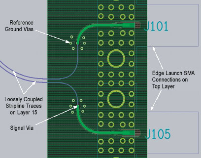
Use tight coupling for differential traces as much as possible. If it is not possible to maintain tight coupling throughout the trace length, use loose coupling for the entire trace. Figure 7 shows 3.125-Gbps differential transceiver traces, which are loosely coupled on layer 15 and the top layer of the Stratix® GX development board. Tight coupling is not possible on the top layer because of the minimum separation required (because of the mechanical constraints of the SMA connectors). If you used tight coupling on layer 15, the signal needs to transition from tight to loose coupling, which introduces impedance discontinuities.
Figure 7. Loose Coupling and Ground Reference Example
- Microstrip and stripline transmission lines are both fine for routing. Stripline has the added benefit of shielding the signals from other noise sources. The constraints during layout design often dictate on which layer to do the routing.
- Use rounded corners while routing. Do not use 90° bends, which introduce impedance discontinuities. A 45° bend provides a compromise, but rounded corners offer the best performance.
- Both broadside and edge coupling are fine. Generally, broadside coupling makes it easy to route out of the BGA, but requires more layers. Edge coupling makes it harder to route out of the BGA, but requires fewer layers. Both provide acceptable signal integrity performance.
- Do not allow high-speed signals to cross over plane splits. A crossover causes signals to see a longer return path, which increases trace inductance. The increased inductance changes the impedance of the line, causing signal integrity problems.
- Remove all unused via pads during the manufacturing process. Some fabrication houses refer to unused via pads as "nonfunctional via pads." Unused via pads add additional capacitance on the signal path. Figure 8 shows examples of unused via pads.
Figure 8. Unused Via Pads
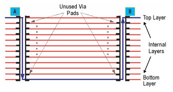
Figure 9. Optimal Routing Path with Through-Hole Vias
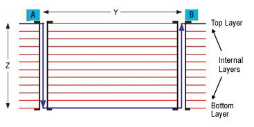
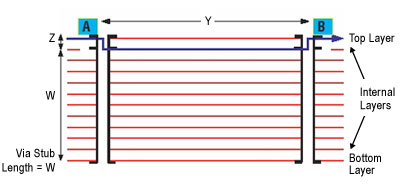
If the signal must be routed through a via, route it so that the via stub length is minimized. The option shown in Figure 9 minimizes the via stub length and is preferred over the option shown in Figure 10. This technique is used in the Stratix® GX development board. The high-speed traces were taken to layer 16 from the top layer through the vias to use as much of the via length as possible and to minimize the stubs.
Figure 10. Sub-Optimal Routing Path with Through-Hole Vias
- For dual stripline traces (Power 1 – Signal 1 – Signal 2 - Power 2 configuration), ensure that the signals on the Signal 1 layer are orthogonal to the signals on the Signal 2 layer if they cross each other. If they do not cross each other, ensure that they are at least 4W away, where W is the width of the traces.
- Use "tear-dropping" to reduce impedance discontinuity when going from a wide pin and trace to a narrow pin or trace. For example, when you interface an SMA connector to a trace, use tear-dropping. Figure 11 shows the dimensions of an SMA connector and a screen capture of tear-dropping on the Stratix® GX development board. The SMA connector has a 50-mil diameter center pin, but the board traces might be 5-mils wide. Tear-dropping helps minimize the impedance discontinuity.
Figure 11. SMA Tear-dropping

Related Information