Visible to Intel only — GUID: joc1463346043115
Ixiasoft
Intel® Stratix® 10 Devices and Transceiver Channels
PCB Stackup Selection Guideline
Recommendations for High Speed Signal PCB Routing
FPGA Fan-out Region Design
CFP2/CFP4 Connector Board Layout Design Guideline
QSFP+/zSFP/QSFP28 Connector Board Layout Design Guideline
SMA 2.4-mm Layout Design Guideline
Tyco/Amphenol Interlaken Connector Design Guideline
Electrical Specifications
Document Revision History for AN 766: Intel® Stratix® 10 Devices, High Speed Signal Interface Layout Design Guideline
Option 1: Via-In-Pad Topology
Option 2: Dog-bone with GND Cutout at BGA Pad Topology
Option 3: Micro-via Topology
GND Cutout Under BGA Pads in Fan-out Configuration
Comparison of Dog-bone with GND Cutout Under the BGA and Via-in-Pad Configurations
Trace Shape Routing at the BGA Void Area (Tear Drop Configuration)
Visible to Intel only — GUID: joc1463346043115
Ixiasoft
CFP4 Connector Layout: Signal Via, Trace Routing Impact, and Optimization
This design example shows the impact of a via anti-pad diameter, trace width at the void area, and the main transmission line impedance at the CFP4 connector. Traditional designs for signal via anti-pad at CFP4 have been for a 50 mil diameter. Reducing via anti-pad diameter to 40 mil shows more impedance matching and less reflection. Changing the trace width on the void area also enhances TDR, IL, and RL performances. Combining both these approaches to reduce the signal via anti-pad diameter and increase the trace width on the void area eventually improves reflections in this area. As mentioned in the fan-out for a 90Ω TL routing impedance, you can see the results of this approach at the connector to see the impact on IL and RL.
Figure 55. Original and Optimized Anti-pad, Trace Width, and TL Impedance Configurations at the CFP4 Connector Area on the PCB
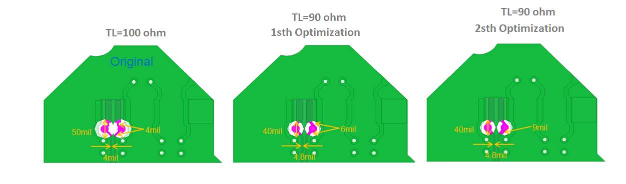
Figure 56. TDR and Full Channel IL and RL Performances Original and optimized anti-pad, trace width, and TL impedance configurations and the CFP4 connector area on the PCB.
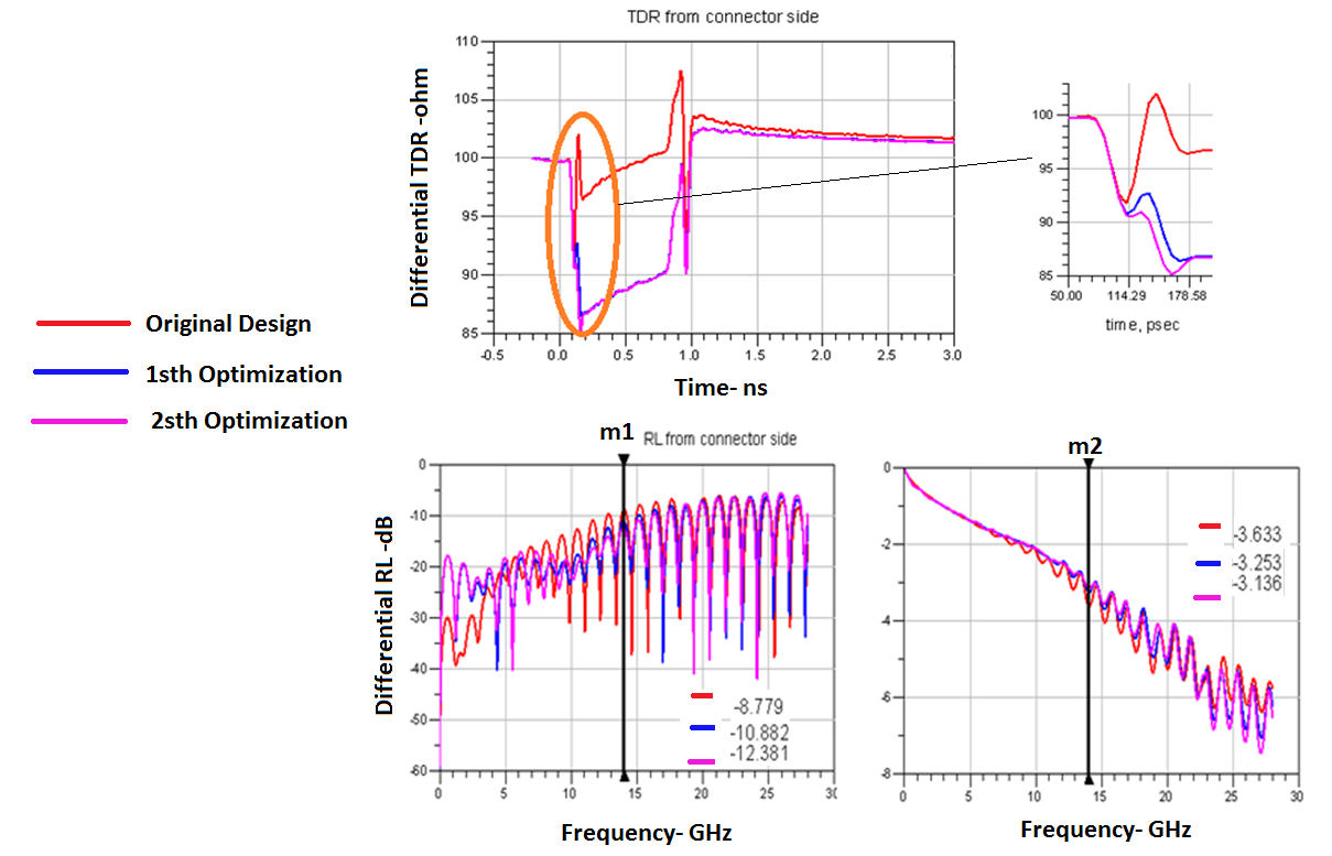
The red line indicates a 4 mil trace width on the void area with a 50 mil anti-pad, and 100Ω TL impedance.
The dark blue line indicates a 6 mil trace width on the void area with a 40 mil anti-pad, and a 90Ω TL impedance.
The pink line indicates a 9 mil trace width on the void area with a 40 mil anti-pad, and a 90Ω TL impedance.
The IL and RL improvement is about 0.5 dB and 3.6 dB at 14 GHz, respectively.