Visible to Intel only — GUID: bdw1484178260761
Ixiasoft
1. Overview
2. Implementing the Transceiver PHY Layer in L-Tile/H-Tile
3. PLLs and Clock Networks
4. Resetting Transceiver Channels
5. Intel® Stratix® 10 L-Tile/H-Tile Transceiver PHY Architecture
6. Reconfiguration Interface and Dynamic Reconfiguration
7. Calibration
8. Debugging Transceiver Links
A. Logical View of the L-Tile/H-Tile Transceiver Registers
2.1. Transceiver Design IP Blocks
2.2. Transceiver Design Flow
2.3. Configuring the Native PHY IP Core
2.4. Using the Intel® Stratix® 10 L-Tile/H-Tile Transceiver Native PHY Intel® Stratix® 10 FPGA IP Core
2.5. Implementing the PHY Layer for Transceiver Protocols
2.6. Unused or Idle Transceiver Channels
2.7. Simulating the Native PHY IP Core
2.8. Implementing the Transceiver Native PHY Layer in L-Tile/H-Tile Revision History
2.3.1. Protocol Presets
2.3.2. GXT Channels
2.3.3. General and Datapath Parameters
2.3.4. PMA Parameters
2.3.5. PCS-Core Interface Parameters
2.3.6. Analog PMA Settings Parameters
2.3.7. Enhanced PCS Parameters
2.3.8. Standard PCS Parameters
2.3.9. PCS Direct Datapath Parameters
2.3.10. Dynamic Reconfiguration Parameters
2.3.11. Generation Options Parameters
2.3.12. PMA, Calibration, and Reset Ports
2.3.13. PCS-Core Interface Ports
2.3.14. Enhanced PCS Ports
2.3.15. Standard PCS Ports
2.3.16. Transceiver PHY PCS-to-Core Interface Reference Port Mapping
2.3.17. IP Core File Locations
2.4.2.1. Receiver Word Alignment
2.4.2.2. Receiver Clock Compensation
2.4.2.3. Encoding/Decoding
2.4.2.4. Running Disparity Control and Check
2.4.2.5. FIFO Operation for the Enhanced PCS
2.4.2.6. Polarity Inversion
2.4.2.7. Data Bitslip
2.4.2.8. Bit Reversal
2.4.2.9. Byte Reversal
2.4.2.10. Double Rate Transfer Mode
2.4.2.11. Asynchronous Data Transfer
2.4.2.12. Low Latency
2.5.1.1. Transceiver Channel Datapath for PIPE
2.5.1.2. Supported PIPE Features
2.5.1.3. How to Connect TX PLLs for PIPE Gen1, Gen2, and Gen3 Modes
2.5.1.4. How to Implement PCI Express (PIPE) in Intel® Stratix® 10 Transceivers
2.5.1.5. Native PHY IP Core Parameter Settings for PIPE
2.5.1.6. fPLL IP Core Parameter Settings for PIPE
2.5.1.7. ATX PLL IP Core Parameter Settings for PIPE
2.5.1.8. Native PHY IP Core Ports for PIPE
2.5.1.9. fPLL Ports for PIPE
2.5.1.10. ATX PLL Ports for PIPE
2.5.1.11. Preset Mappings to TX De-emphasis
2.5.1.12. How to Place Channels for PIPE Configurations
2.5.1.13. Link Equalization for Gen3
2.5.1.14. Timing Closure Recommendations
3.1. PLLs
3.2. Input Reference Clock Sources
3.3. Transmitter Clock Network
3.4. Clock Generation Block
3.5. FPGA Fabric-Transceiver Interface Clocking
3.6. Double Rate Transfer Mode
3.7. Transmitter Data Path Interface Clocking
3.8. Receiver Data Path Interface Clocking
3.9. Channel Bonding
3.10. PLL Cascading Clock Network
3.11. Using PLLs and Clock Networks
3.12. PLLs and Clock Networks Revision History
4.1. When Is Reset Required?
4.2. Transceiver PHY Reset Controller Intel® Stratix® 10 FPGA IP Implementation
4.3. How Do I Reset?
4.4. Using PCS Reset Status Port
4.5. Using Transceiver PHY Reset Controller Intel® Stratix® 10 FPGA IP
4.6. Using a User-Coded Reset Controller
4.7. Combining Status or PLL Lock Signals with User Coded Reset Controller
4.8. Resetting Transceiver Channels Revision History
4.3.1.1. Resetting the Transmitter After Power Up
4.3.1.2. Resetting the Transmitter During Device Operation
4.3.1.3. Resetting the Receiver After Power Up
4.3.1.4. Resetting the Receiver During Device Operation (Auto Mode)
4.3.1.5. Clock Data Recovery in Manual Lock Mode
4.3.1.6. Special TX PCS Reset Release Sequence
4.5.1. Parameterizing Transceiver PHY Reset Controller Intel® Stratix® 10 FPGA IP
4.5.2. Transceiver PHY Reset Controller Intel® Stratix® 10 FPGA IP Parameters
4.5.3. Transceiver PHY Reset Controller Intel® Stratix® 10 FPGA IP Interfaces
4.5.4. Transceiver PHY Reset Controller Intel® Stratix® 10 FPGA IP Resource Utilization
5.1. PMA Architecture
5.2. Enhanced PCS Architecture
5.3. Intel® Stratix® 10 Standard PCS Architecture
5.4. Intel® Stratix® 10 PCI Express Gen3 PCS Architecture
5.5. PCS Support for GXT Channels
5.6. Square Wave Generator
5.7. PRBS Pattern Generator
5.8. PRBS Pattern Verifier
5.9. Loopback Modes
5.10. Intel® Stratix® 10 L-Tile/H-Tile Transceiver PHY Architecture Revision History
5.1.2.1.1. Programmable Differential On-Chip Termination (OCT)
5.1.2.1.2. Signal Detector
5.1.2.1.3. Continuous Time Linear Equalization (CTLE)
5.1.2.1.4. Variable Gain Amplifier (VGA)
5.1.2.1.5. Adaptive Parametric Tuning (ADAPT) Engine
5.1.2.1.6. Decision Feedback Equalization (DFE)
5.1.2.1.7. On-Die Instrumentation
5.2.1.1. TX Core FIFO
5.2.1.2. TX PCS FIFO
5.2.1.3. Interlaken Frame Generator
5.2.1.4. Interlaken CRC-32 Generator
5.2.1.5. 64B/66B Encoder and Transmitter State Machine (TX SM)
5.2.1.6. Scrambler
5.2.1.7. Interlaken Disparity Generator
5.2.1.8. TX Gearbox, TX Bitslip and Polarity Inversion
5.2.1.9. KR FEC Blocks
5.2.2.1. RX Gearbox, RX Bitslip, and Polarity Inversion
5.2.2.2. Block Synchronizer
5.2.2.3. Interlaken Disparity Checker
5.2.2.4. Descrambler
5.2.2.5. Interlaken Frame Synchronizer
5.2.2.6. 64B/66B Decoder and Receiver State Machine (RX SM)
5.2.2.7. 10GBASE-R Bit-Error Rate (BER) Checker
5.2.2.8. Interlaken CRC-32 Checker
5.2.2.9. RX PCS FIFO
5.2.2.10. RX Core FIFO
5.3.1.4.1. 8B/10B Encoder Control Code Encoding
5.3.1.4.2. 8B/10B Encoder Reset Condition
5.3.1.4.3. 8B/10B Encoder Idle Character Replacement Feature
5.3.1.4.4. 8B/10B Encoder Current Running Disparity Control Feature
5.3.1.4.5. 8B/10B Encoder Bit Reversal Feature
5.3.1.4.6. 8B/10B Encoder Byte Reversal Feature
5.3.2.1.1. Word Aligner Bitslip Mode
5.3.2.1.2. Word Aligner Manual Mode
5.3.2.1.3. Word Aligner Synchronous State Machine Mode
5.3.2.1.4. Word Aligner Deterministic Latency Mode
5.3.2.1.5. Word Aligner Pattern Length for Various Word Aligner Modes
5.3.2.1.6. Word Aligner RX Bit Reversal Feature
5.3.2.1.7. Word Aligner RX Byte Reversal Feature
5.3.2.6.1. Byte Deserializer Disabled Mode
5.3.2.6.2. Byte Deserializer Deserialize x2 Mode
5.3.2.6.3. Byte Deserializer Deserialize x4 Mode
5.3.2.6.4. Bonded Byte Deserializer
5.3.2.6.5. Byte Ordering Register-Transfer Level (RTL)
5.3.2.6.6. Byte Serializer Effects on Data Propagation at the RX Side
5.3.2.6.7. ModelSim Byte Ordering Analysis
6.1. Reconfiguring Channel and PLL Blocks
6.2. Interacting with the Reconfiguration Interface
6.3. Multiple Reconfiguration Profiles
6.4. Arbitration
6.5. Recommendations for Dynamic Reconfiguration
6.6. Steps to Perform Dynamic Reconfiguration
6.7. Direct Reconfiguration Flow
6.8. Native PHY IP or PLL IP Core Guided Reconfiguration Flow
6.9. Reconfiguration Flow for Special Cases
6.10. Changing Analog PMA Settings
6.11. Ports and Parameters
6.12. Dynamic Reconfiguration Interface Merging Across Multiple IP Blocks
6.13. Embedded Debug Features
6.14. Timing Closure Recommendations
6.15. Unsupported Features
6.16. Transceiver Register Map
6.17. Reconfiguration Interface and Dynamic Revision History
7.5.1. Recalibrating a Duplex Channel (Both PMA TX and PMA RX)
7.5.2. Recalibrating the PMA RX Only in a Duplex Channel
7.5.3. Recalibrating the PMA TX Only in a Duplex Channel
7.5.4. Recalibrating a PMA Simplex RX Without a Simplex TX Merged into the Same Physical Channel
7.5.5. Recalibrating a PMA Simplex TX Without a Simplex RX Merged into the Same Physical Channel
7.5.6. Recalibrating Only a PMA Simplex RX in a Simplex TX Merged Physical Channel
7.5.7. Recalibrating Only a PMA Simplex TX in a Simplex RX Merged Physical Channel
7.5.8. Recalibrating the fPLL
7.5.9. Recalibrating the ATX PLL
7.5.10. Recalibrating the CMU PLL When it is Used as a TX PLL
A.4.1. Transmitter PMA Logical Register Map
A.4.2. Receiver PMA Logical Register Map
A.4.3. Pattern Generators and Checkers
A.4.4. Loopback
A.4.5. Optional Reconfiguration Logic PHY- Capability
A.4.6. Optional Reconfiguration Logic PHY- Control & Status
A.4.7. Embedded Streamer (Native PHY)
A.4.8. Static Polarity Inversion
A.4.9. Reset
A.4.10. CDR/CMU and PMA Calibration
Visible to Intel only — GUID: bdw1484178260761
Ixiasoft
7. Calibration
Transceivers include both analog and digital blocks that require calibration to compensate for process, voltage, and temperature (PVT) variations. Intel® Stratix® 10 transceivers use hardened Precision Signal Integrity Calibration Engine (PreSICE) to perform calibration routines. Each transceiver tile has a PreSICE engine. If you are using more than 24 transceiver channels in your design, the transceiver calibrates on a per tile basis. This means that channel 0 in tile 1 and channel 0 in tile 2 are calibrated concurrently, etc.
Power-up Calibration, Background Calibration and User Recalibration are the main types of calibration.
- Power-up calibration occurs automatically at device power-up. It runs during device configuration.
- After you enable background calibration, background calibration continuously runs in the background.
- Use dynamic reconfiguration to trigger user recalibration. In this case, you are responsible for enabling the required calibration sequence.
Note: Only H-Tile production devices support background calibration.
When you upgrade from a previous version of the Intel® Quartus® Prime software to Intel® Quartus® Prime software version 18.1 or above, the Native PHY IP automatically upgrades any H-tile GXT design transceiver link operating at datarates ≥ 17.5 Gbps to Enable background calibration. Refer to Background Calibration for more information about specific requirements and how to control the background calibration.
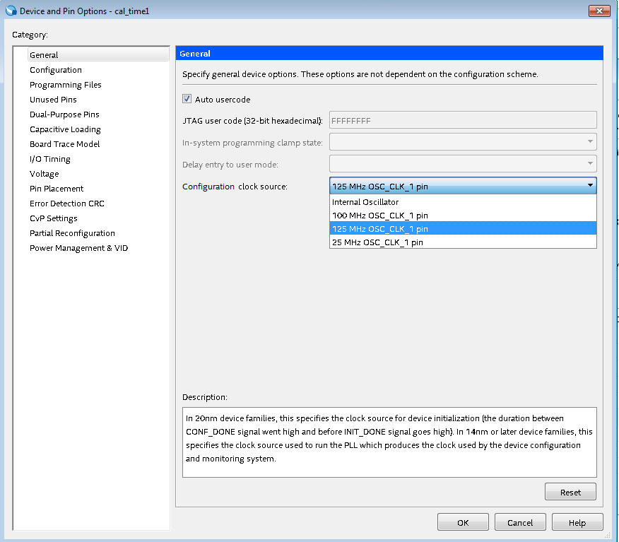
Intel® Stratix® 10 devices use the OSC_CLK_1 pin to provide the transceiver calibration clock source. You must provide a 25, 100, or 125 MHz free running and stable clock to OSC_CLK_1.
The FPGA's Internal Oscillator cannot be used for transceiver calibration. Do not select this clock source as the Configuration clock source in the Intel® Quartus® Prime settings.
In addition to providing this clock, you must also choose the appropriate frequency in Quartus assignments:
Quartus assignments > Device > Device and Pin Options > Configuration clock source
- Scroll down menu
- Choose 25, 100, or 125 MHz OSC_CLK_1 pin option.
Figure 250. Calibration Clock Options
Note:
You see the selected clock source in .qsf as follows:
set_global_assignment -name DEVICE_INITIALIZATION_CLOCK OSC_CLK_1_125MHz
There is a PLL inside the FPGA that receives the clock from OSC_CLK_1 and provides a 250-MHz calibration clock to PreSICE. All reference clocks driving transceiver PLLs (ATX PLL, fPLL, CDR/CMU PLL) must have a stable frequency and be free running before the start of FPGA configuration (pull the FPGA’s nCONFIG input high). For more information about OSC_CLK_1 pin requirements, refer to the Intel® Stratix® 10 GX and SX Device Family Pin Connection Guidelines.