1.4. Compiling and Testing the Design in Hardware
Figure 8. Compiling and Testing the Design Flow
To compile and run a demonstration test on the hardware design example, follow these steps:
- Open the Intel® Quartus® Prime project (sdi_ii_agi_demo.qpf) located in Quartus directory.
- To perform Intel® Quartus® Prime compilation, click .
- Connects the Nextera SDI daughter card to FMC port A on the development kit.
- For parallel loopback design, connects the BNC RX connector (J1/12G In) to an external video source and connects the TX connector (J2/12G Out) to a video analyzer. For serial loopback design, connects the BNC TX connector (J2/12G Out) to RX connector (J1/12G In) or a video analyzer.
- Ensure all the switches on the development kit are in their default position.
If you are generating parallel loopback without external VCXO design example, or you have enabled the Dynamic Tx clock switching parameter, toggle DIPSW S22.3 onboard to OFF position
- Open Clock Controller GUI and navigate to Si5391-A tab, set Out9 frequency to:
- Parallel loopback without external VCXO – 140.00000 MHz
- Dynamic Tx clock switching is enabled – 148.35160 MHz
Figure 9. Setting Out9 frequency in Clock Controller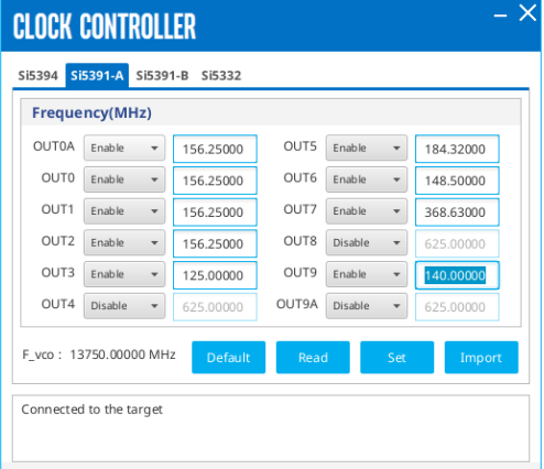
- After the compilation completes, open Programmer and program the generated .sof file to the development kit.
- For serial loopback design, you need to open System Console to control the internal video pattern generator.
- Go to and click System Console.
- After the initialization, type source ../hwtest/tpg_ctrl.tcl to open the pattern generator control UI.
- Select your desired video format through the UI.
Note: To allow segmented frame video format (1080sF30, 1080sF25) and interlaced video format (1080i60, 1080i50) to be correctly differentiated in external analyzer, you must insert Payload ID in the serial loopback designFigure 10. Selecting Video Format Through System Console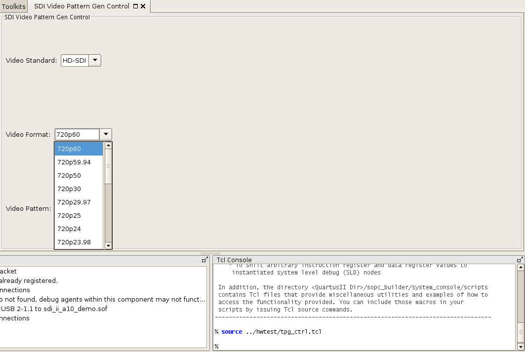
- The analyzer should be able to display the video generated from the source. Refer to jumper settings in the Jumper Settings and Descriptions Table to change the jumper (J8) position before switching between fractional frame rate and integer frame rate video format. You must press the push button (PB0) to trigger a device (LMK03328) power cycling through the PDN pin every time you change the jumper (J8) position.
Figure 11. Jumper Settings on Nextera 12G-SDI FMC Daughtercard
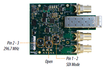
| Jumper Block | Description | Setting |
|---|---|---|
| J7 | Programming Header | - |
| J8 | To switch the generated clock frequency to TX channel:
|
1-2: 297 Mhz 2-3: 297/1.001 Mhz |
| J9 | To select SDI or IP mode:
|
1-2 |