Visible to Intel only — GUID: awv1638889111075
Ixiasoft
1. About this Document
2. Introduction
3. Nios® V Processor Hardware System Design with Intel® Quartus® Prime Pro Edition and Platform Designer
4. Nios® V Processor Software System Design
5. Nios® V Processor Configuration and Booting Solutions
6. Nios® V Processor - Using the MicroC/TCP-IP Stack
7. Nios® V Processor Debugging, Verifying, and Simulating
8. Document Revision History for the Nios® V Embedded Processor Design Handbook
5.1. Introduction
5.2. Linking Applications
5.3. Nios® V Processor Booting Methods
5.4. Introduction to Nios® V Processor Booting Methods
5.5. Nios® V Processor Booting from Configuration QSPI Flash
5.6. Nios V Processor Booting from On-Chip Memory (OCRAM)
5.7. Summary of Nios V Processor Vector Configuration and BSP Settings
5.5.2.1.1. Hardware Design Flow
IP Component Settings
Reset and Exception Agent Settings for Nios Processor
Intel Quartus Prime Software Settings
5.5.2.1.2. Software Design Flow
5.5.2.1.3. Software Design Flow (SDM Bootloader Project)
5.5.2.1.4. Software Design Flow (User Application Project)
5.5.2.1.5. Programming Files Generation
5.5.2.1.6. QSPI Flash Programming SDM
7.4.1. Prerequisites
7.4.2. Setting Up and Generating Your Simulation Environment in Platform Designer
7.4.3. Creating Nios V Processor Software
7.4.4. Generating Memory Initialization File
7.4.5. Generating System Simulation Files
7.4.6. Running Simulation in the QuestaSim Simulator Using Command Line
Visible to Intel only — GUID: awv1638889111075
Ixiasoft
5.5.2.1.1. Hardware Design Flow
The following sections describe a step-by-step method for building a bootable system for a Nios V processor application copied from configuration QSPI flash to RAM using SDM Bootloader. The example below is built using Intel Stratix 10 SX SoC L-Tile.
IP Component Settings
- Create your Nios® V processor project using Intel® Quartus® Prime and Platform Designer.
- Add the Mailbox Client Intel® FPGA IP into your Platform Designer system.
Figure 47. Connections for Nios V Processor ProjectFigure 48. On-Chip Memory (RAM or ROM) Intel FPGA IP Parameter Settings
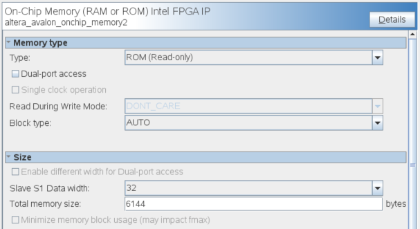
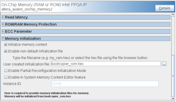
- Change the On-Chip Memory (RAM or ROM) Intel FPGA IP Parameter Settings according to the memory function. Check that you have a total of four memories in the system.
| Memory | Memory Type | Total Memory Size | Memory initialization |
|---|---|---|---|
| Bootloader ROM | ROM (Read-only) |
6144 bytes or more |
Enable the following settings:
|
| Bootloader RAM | RAM (Writable) |
6144 bytes or more |
Leave all settings unchecked. |
| User Application RAM | RAM (Writable) |
Depends on your application 9 |
Leave all settings unchecked. |
| Exception RAM | RAM (Writable) |
Depends on your application 9 |
Leave all settings unchecked. |
Reset and Exception Agent Settings for Nios Processor
- In the Nios V Processor parameter editor, set the Reset Agent to Bootloader ROM and Exception Agent to Exception RAM.
Figure 49. Nios V Parameter Editor Settings
- Click Generate HDL, the Generation dialog box appears.
- Specify output file generation options and then click Generate.
Intel Quartus Prime Software Settings
- In the Intel Quartus Prime software, click Assignment > Device > Device and Pin Options > Configuration.
- Set Configuration scheme to Active Serial x4 (can use Configuration Device).
- Set VID mode of operation according to your board design.
- Set the Active serial clock source to 100 MHz Internal Oscillator.
Figure 50. Device and Pin Options
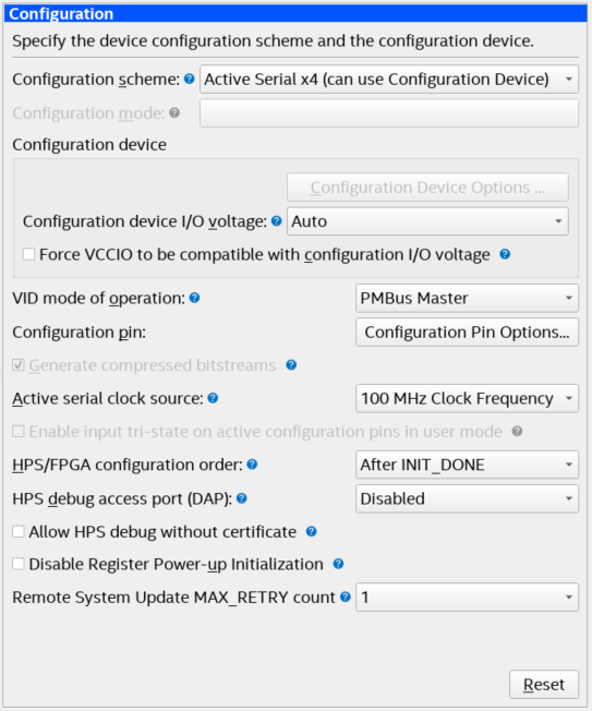
- Click OK to exit the Device and Pin Options window.
- Click OK to exit the Device window.
- Click Start Compilation to compile your project.
9 Your application size varies according to the usage. Set the memory size according to your design.