Visible to Intel only — GUID: osa1651157203680
Ixiasoft
1. About the Video and Vision Processing Suite
2. Getting Started with the Video and Vision Processing IPs
3. Video and Vision Processing IPs Functional Description
4. Video and Vision Processing IP Interfaces
5. Video and Vision Processing IP Registers
6. Video and Vision Processing IPs Software Programming Model
7. Protocol Converter Intel® FPGA IP
8. 1D LUT Intel® FPGA IP
9. 3D LUT Intel® FPGA IP
10. AXI-Stream Broadcaster Intel® FPGA IP
11. Bits per Color Sample Adapter Intel FPGA IP
12. Black Level Correction Intel® FPGA IP
13. Black Level Statistics Intel® FPGA IP
14. Chroma Key Intel® FPGA IP
15. Chroma Resampler Intel® FPGA IP
16. Clipper Intel® FPGA IP
17. Clocked Video Input Intel® FPGA IP
18. Clocked Video to Full-Raster Converter Intel® FPGA IP
19. Clocked Video Output Intel® FPGA IP
20. Color Plane Manager Intel® FPGA IP
21. Color Space Converter Intel® FPGA IP
22. Defective Pixel Correction Intel® FPGA IP
23. Deinterlacer Intel® FPGA IP
24. Demosaic Intel® FPGA IP
25. FIR Filter Intel® FPGA IP
26. Frame Cleaner Intel® FPGA IP
27. Full-Raster to Clocked Video Converter Intel® FPGA IP
28. Full-Raster to Streaming Converter Intel® FPGA IP
29. Genlock Controller Intel® FPGA IP
30. Generic Crosspoint Intel® FPGA IP
31. Genlock Signal Router Intel® FPGA IP
32. Guard Bands Intel® FPGA IP
33. Histogram Statistics Intel® FPGA IP
34. Interlacer Intel® FPGA IP
35. Mixer Intel® FPGA IP
36. Pixels in Parallel Converter Intel® FPGA IP
37. Scaler Intel® FPGA IP
38. Stream Cleaner Intel® FPGA IP
39. Switch Intel® FPGA IP
40. Tone Mapping Operator Intel® FPGA IP
41. Test Pattern Generator Intel® FPGA IP
42. Unsharp Mask Intel® FPGA IP
43. Video and Vision Monitor Intel FPGA IP
44. Video Frame Buffer Intel® FPGA IP
45. Video Frame Reader Intel FPGA IP
46. Video Frame Writer Intel FPGA IP
47. Video Streaming FIFO Intel® FPGA IP
48. Video Timing Generator Intel® FPGA IP
49. Vignette Correction Intel® FPGA IP
50. Warp Intel® FPGA IP
51. White Balance Correction Intel® FPGA IP
52. White Balance Statistics Intel® FPGA IP
53. Design Security
54. Document Revision History for Video and Vision Processing Suite User Guide
29.4.1. Achieving Genlock Controller Free Running (for Initialization or from Lock to Reference Clock N)
29.4.2. Locking to Reference Clock N (from Genlock Controller IP free running)
29.4.3. Setting the VCXO hold over
29.4.4. Restarting the Genlock Controller IP
29.4.5. Locking to Reference Clock N New (from Locking to Reference Clock N Old)
29.4.6. Changing to Reference Clock or VCXO Base Frequencies (switch between p50 and p59.94 video formats and vice-versa)
29.4.7. Disturbing a Reference Clock (a cable pull)
Visible to Intel only — GUID: osa1651157203680
Ixiasoft
23.2. Deinterlacer Parameters
The IP offers run- and compile-time parameters.
| Parameter | Values | Description |
|---|---|---|
| Parameters | ||
| Deinterlacing mode | Bob or Weave | Select bob or weave deinterlacer. |
| Video Data Format | ||
| Bits per color sample | 8 to 16 | Select the number of bits per color sample. |
| Number of color planes | 1 to 4 | Select the number of color planes per pixel. |
| Number of pixels in parallel | 1 to 8 | Select the number of pixels in parallel. |
| Memory 58 | ||
| Avalon memory- mapped host(s) local ports width | 16, 32, 64, 128, 256, 512, 1024 | Select in bits the width of the Avalon memory-mapped host read and write ports. |
| Avalon memory- mapped host(s) local ports address width | 8 to 32 | Select in bits the width of the Avalon memory-mapped host read and write ports. It must be sufficient to fully address the last buffer. |
| The depth of the write FIFO | 32, 64, 128, 256, 512, 1024, 2048 | Select the depth of the write FIFO buffer. Each FIFO buffer entry holds one word the width of the specified Avalon memory-mapped local port width. You must specify a FIFO depth of at least twice the specified burst target so that at least 2 bursts can be held at any one time. Increase the FIFO depth to improve resilience to latency on the Avalon memory-mapped bus. |
| Avalon memory- mapped write burst target | 2,4,8,16,32,64 | Select the burst target for writes. Longer bursts provide more efficiency on the bus but require more local storage in the write FIFO buffer. |
| The depth of the read FIFO | 32,64,128,256,512,1024,2048 | Specify the depth of the read FIFO buffer. Each FIFO buffer entry holds one word the width of the specified Avalon memory-mapped local port width. You must specify a FIFO depth of at least twice the specified burst target so that at least 2 bursts can be held at any one time. Increase the FIFO depth to improve resilience to latency on the Avalon memory-mapped bus. |
| Avalon memory- mapped read burst target | 2,4,8,16,32,64 | Select the burst target for reads. Longer bursts provide more efficiency on the bus but require more local storage in the read FIFO buffer. |
| Field memory base address | 0x0000_0000 – 0x7FFF_FFFF | Select the base address for the field buffer to store field 0 or field 1. |
| Interline stride | Depends on video frame format and maximum frame width. | Set a stride (in bytes) large enough to separate lines of the specified maximum width. The GUI gives an error if the stride is too low. |
| Packing method | Perfect, color or pixel | Perfect packing minimizes memory footprint of stored fields but increases complexity and therefore size of the field buffer slightly. Color packing leaves spaces in memory between colors if colors do not pack into memory words exactly. Pixel packing leaves spaces in memory between pixels if pixels do not pack into memory words exactly. |
| Separate clock for the Avalon memory- mapped host interface(s) | On or off | A separate clock allows the control and data portions of the field buffer to run at their maximum clock frequencies. Turn on separate clocks for highest performance. |
| Control | ||
| Lite mode | On or off | Turn on to operate the deinterlacer in lite mode. |
| Memory-mapped control interface | On or off | Turn on to read frame statistics and turn the deinterlacer on and off using an Avalon memory-mapped interface. The memory-mapped control interface is mandatory in lite mode. |
| Separate clock for control interface | On or off | Turn on for a separate clock for the control interface. |
| Deinterlacer Behavior 59 | ||
| Bob deinterlacing mode | DEINTERLACE_F0_ONLY, DEINTERLACE_F1_ONLY, DEINTERLACE_F0_AND_F1 |
Select to drop off F0 or F1 input fields. |
| Maximum Frame Size | ||
| Maximum field width | 32 to 16384 | Select the maximum field width to determine the size of the line buffer. Set this parameter to the line length of the widest fields you want to deinterlace. Progressive frames of any size pass through unchanged. |
| General | ||
| Debug features | On or off | Turn on to enable debug features (not applicable for lite mode). |
| Pipeline ready signals | On or off | Turn on to add extra pipeline registers to the AXI4-S tready signals |
| Use FIFO | On or off | Add optional FIFO buffer. |
Figure 60. Deinterlacer GUI
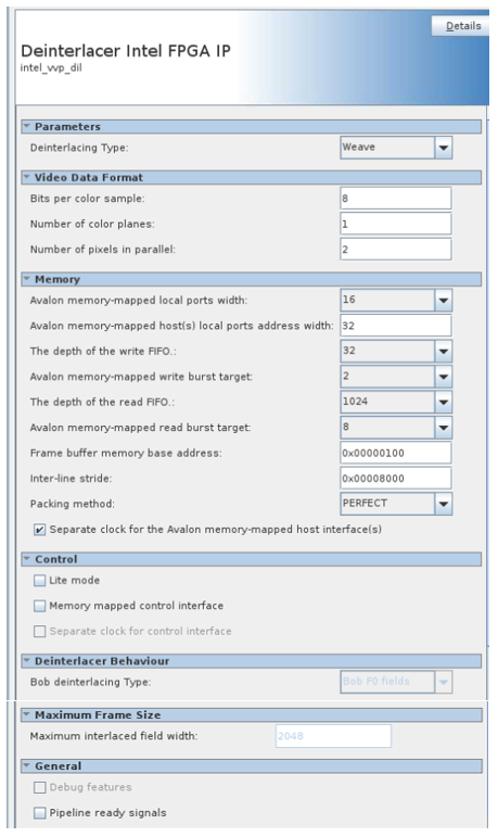
Figure 61. Bob DeinterlacingThe figure shows the bob deinterlacing where the IP drops or deinterlaces interlaced fields. The IP passes all progressive frames through.
Figure 62. Weave Interlacing
The figure shows the weave deinterlacing, where the IP drops or deinterlaces interlaced fields. The IP passes all progressive frames through. For incoming F1 and F0, the weave deinterlacer deinterlaces or drops the fields based on the nibble values. For more information on nibble, refer to the Intel FPGA Streaming Video Protocol Specification.
58 Only for weave deinterlacer
59 Bob deinterlacer only