Visible to Intel only — GUID: qff1684241111615
Ixiasoft
1. About the Video and Vision Processing Suite
2. Getting Started with the Video and Vision Processing IPs
3. Video and Vision Processing IPs Functional Description
4. Video and Vision Processing IP Interfaces
5. Video and Vision Processing IP Registers
6. Video and Vision Processing IPs Software Programming Model
7. Protocol Converter Intel® FPGA IP
8. 1D LUT Intel® FPGA IP
9. 3D LUT Intel® FPGA IP
10. AXI-Stream Broadcaster Intel® FPGA IP
11. Bits per Color Sample Adapter Intel FPGA IP
12. Black Level Correction Intel® FPGA IP
13. Black Level Statistics Intel® FPGA IP
14. Chroma Key Intel® FPGA IP
15. Chroma Resampler Intel® FPGA IP
16. Clipper Intel® FPGA IP
17. Clocked Video Input Intel® FPGA IP
18. Clocked Video to Full-Raster Converter Intel® FPGA IP
19. Clocked Video Output Intel® FPGA IP
20. Color Plane Manager Intel® FPGA IP
21. Color Space Converter Intel® FPGA IP
22. Defective Pixel Correction Intel® FPGA IP
23. Deinterlacer Intel® FPGA IP
24. Demosaic Intel® FPGA IP
25. FIR Filter Intel® FPGA IP
26. Frame Cleaner Intel® FPGA IP
27. Full-Raster to Clocked Video Converter Intel® FPGA IP
28. Full-Raster to Streaming Converter Intel® FPGA IP
29. Genlock Controller Intel® FPGA IP
30. Generic Crosspoint Intel® FPGA IP
31. Genlock Signal Router Intel® FPGA IP
32. Guard Bands Intel® FPGA IP
33. Histogram Statistics Intel® FPGA IP
34. Interlacer Intel® FPGA IP
35. Mixer Intel® FPGA IP
36. Pixels in Parallel Converter Intel® FPGA IP
37. Scaler Intel® FPGA IP
38. Stream Cleaner Intel® FPGA IP
39. Switch Intel® FPGA IP
40. Tone Mapping Operator Intel® FPGA IP
41. Test Pattern Generator Intel® FPGA IP
42. Unsharp Mask Intel® FPGA IP
43. Video and Vision Monitor Intel FPGA IP
44. Video Frame Buffer Intel® FPGA IP
45. Video Frame Reader Intel FPGA IP
46. Video Frame Writer Intel FPGA IP
47. Video Streaming FIFO Intel® FPGA IP
48. Video Timing Generator Intel® FPGA IP
49. Vignette Correction Intel® FPGA IP
50. Warp Intel® FPGA IP
51. White Balance Correction Intel® FPGA IP
52. White Balance Statistics Intel® FPGA IP
53. Design Security
54. Document Revision History for Video and Vision Processing Suite User Guide
29.4.1. Achieving Genlock Controller Free Running (for Initialization or from Lock to Reference Clock N)
29.4.2. Locking to Reference Clock N (from Genlock Controller IP free running)
29.4.3. Setting the VCXO hold over
29.4.4. Restarting the Genlock Controller IP
29.4.5. Locking to Reference Clock N New (from Locking to Reference Clock N Old)
29.4.6. Changing to Reference Clock or VCXO Base Frequencies (switch between p50 and p59.94 video formats and vice-versa)
29.4.7. Disturbing a Reference Clock (a cable pull)
Visible to Intel only — GUID: qff1684241111615
Ixiasoft
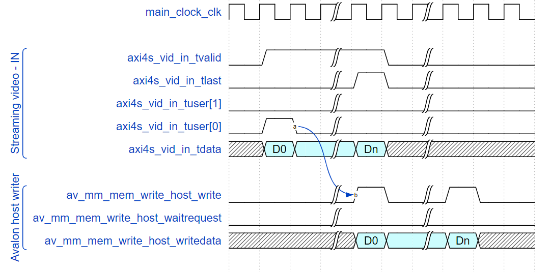
46.3. Video Frame Writer IP Functional Description
The IP receives video fields or frames from its Intel FPGA streaming video input and writes them to external memory via its Avalon memory-mapped interface.
- Configure the IP with the number of buffers that you want to write to with the csr_num_buffers register.
- Program the base address in memory for the first buffer, the offset between buffers and the offset between individual lines within buffers via the csr_buffer_base, csr_inter_buffer_offset and csr_inter_line_offset registers.
- Set the csr_overwrite_broken register if you want broken frames to be overwritten and then csr_run to either free-running mode for continuous operation or single-shot mode.
- Commit these settings with a write to the csr_commit register.
If the IP receives any packets on its Intel FPGA streaming video input before you configure and commit it, the IP consumes the packets. When consuming, the IP raises axi4s_vid_in_tready.
Register Behavior
Bit [0] of the csr_status register goes high when the IP starts writing the first frame. It goes low after the IP finishes writing the last line of the frame. It returns high when the IP starts writing the next frame.
The IP sets the csr_buffer_available register after it writes the first frame and a buffer is available in memory. csr_buffer_start_address holds the base address of the first frame and csr_buffer_write_count increments with each frame the IP writes. If the IP receives an interlaced f1 field, it sets csr_buffer_f1_flag. The IP sets csr_buffer_field_width and csr_buffer_field_height to the dimensions of the new value. In full mode, the IP extracts the field count from each end of field packet and updatescsr_field_count.
Acknowledge the buffer by writing to the csr_buffer_acknowledge register, which resets csr_buffer_available. If you do not acknowledge the buffer, csr_buffer_available remains set, the IP keeps writing frames and csr_buffer_start_address and associated registers update as normal.
Latency
The frame writer latency depends on the availability of the external memory interfaces, which may create backpressure for the IP’s write interface via the av_mm_mem_read_host_waitrequest signal.
The worst-case latency figures are when the frame writer experiences no backpressure. Any backpressure increases these latencies by the same amount of cycles.
The latency figures are for when the host interfaces do not have a separate clock, so all interfaces operate from the same clock.
The latency figures are for a typical configuration. Reducing the burst target reduces latency but at the cost of decreasing efficiency and increasing bandwidth consumed on the bus.
| Initiating event | Resultant event | Latency (measured in clock cycles) |
|---|---|---|
| axi4s_vid_in_tuser[0] strobe to indicate start of frame | First av_mm_mem_write_host_write strobe of a frame write | 44 |
Figure 115. Latency